Web Analytics
Part Datasheet Search > Shift Registers > MC14094 Datasheet PDF
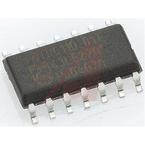
Images are for reference

MC14094 Datasheet PDF

Part Series:
MC14094 Series
Category:
Shift Registers
Description:
ON SEMICONDUCTOR MC14094BDR2G Shift Register, MC14094, Serial to Parallel, 1Element, 8Bit, SOIC, 16Pins
Updated Time: 2023/01/13 02:46:09 (UTC + 8)

MC14094 Shift Registers Datasheet PDF

MC14094 Datasheet PDF Shift Registers

11 Pages
ON Semiconductor
Shift Register/Latch Single 8Bit Serial to Serial/Parallel Automotive 16Pin PDIP Tube
11 Pages
ON Semiconductor
Shift Register/Latch Single 8Bit Serial to Serial/Parallel 16Pin SOIC Rail
11 Pages
ON Semiconductor
Counter Shift Registers 3-18V 8Bit
10 Pages
ON Semiconductor
ON SEMICONDUCTOR MC14094BDG Shift Register, MC14094, Serial to Parallel, 1Element, 8Bit, SOIC, 16Pins
10 Pages
ON Semiconductor
Counter Shift Registers 3-18V 8Bit Shift/Store
10 Pages
ON Semiconductor
Shift Register/Latch Single 8Bit Serial to Serial/Parallel 16Pin SO EIAJ Rail
9 Pages
ON Semiconductor
Shift Register/Latch Single 8Bit Serial to Serial/Parallel 16Pin SOIC T/R
9 Pages
ON Semiconductor
8Bit Shift/Store Register with Three-State Outputs
9 Pages
Motorola
IC SHIFT REGISTER 8STAGE 16-DIP
9 Pages
ON Semiconductor
Shift Register/Latch Single 8Bit Serial to Serial/Parallel Automotive 16Pin TSSOP

MC14094BDR2G - ON Semiconductor Specifications

TYPE
DESCRIPTION
Mounting Style
Surface Mount
Number of Pins
16 Pin
Supply Voltage (DC)
3.00V (min)
Capacitance
7.5 pF
Case/Package
SOIC-16
show more

MC14094BDR2G - ON Semiconductor Function Overview

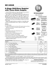
The MC14094B combines an 8−stage shift register with a data latch for each stage and a 3−state output from each latch. Data is shifted on the positive clock transition and is shifted from the seventh stage to two serial outputs. The QSoutput data is for use in high−speed cascaded systems. The QSoutput data is shifted on the following negative clock transition for use in low−speed cascaded systems. Data from each stage of the shift register is latched on the negative transition of the strobe input. Data propagates through the latch while strobe is high. Outputs of the eight data latches are controlled by 3−state buffers which are placed in the high−impedance state by a logic Low on Output Enable.
Features
•3−State Outputs
•Capable of Driving Two Low−Power TTL Loads or One Low−Power Schottky TTL Load Over the Rated Temperature Range
•Input Diode Protection
•Data Latch
•Dual Outputs for Data Out on Both Positive and Negative Clock Transitions
•Useful for Serial−to−Parallel Data Conversion
•Pin−for−Pin Compatible with CD4094B
•These Devices are Pb−Free and are RoHS Compliant
•NLV Prefix for Automotive and Other Applications Requiring Unique Site and Control Change Requirements; AEC−Q100 Qualified and PPAP Capable
show more
Part Datasheet PDF Search
Loading...
72,405,303 Parts Datasheet PDF, Update more than 5,000 PDF files ervery day.
Relate Parts