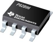
●The P82B96 device is a bus buffer that supports bidirectional data transfer between an I2C bus and a range of other bus configurations with different voltage and current levels.
●One of the advantages of the P82B96 is that it supports longer cables/traces and allows for more devices per I2C bus because it can isolate bus capacitance such that the total loading (devices and trace lengths) of the new bus or remote I2C nodes are not apparent to other I2C buses (or nodes). The restrictions on the number of I2C devices in a system due to capacitance, or the physical separation between them, are greatly improved.
●The device is able to provide galvanic isolation (optocoupling) or use balanced transmission lines (twisted pairs), because separate directional Tx and Rx signals are provided. The Tx and Rx signals may be connected directly (without causing bus latching), to provide an bidirectional signal line with I2C properties (open-drain driver). Likewise, the Ty and Ry signals may also be connected together to provide an bidirectional signal line with I2C properties (open-drain driver). This allows for a simple communication design, saving design time and costs.
●Two or more Sx or Sy I/Os must not be connected to each other on the same node. The P82B96 design does not support this configuration. Bidirectional I2C signals do not have a direction control pin so, instead, slightly different logic low-voltage levels are used at Sx/Sy to avoid latching of this buffer. A standard I2C low applied at the Rx/Ry of a P82B96 is propagated to Sx/Sy as a buffered low with a slightly higher voltage level. If this special buffered low is applied to the Sx/Sy of another P82B96, the second P82B96 does not recognize it as a standard I2C bus low and does not propagate it to its Tx/Ty output. The Sx/Sy side of P82B96 may not be connected to similar buffers that rely on special logic thresholds for their operation.
●The Sx/Sy side of the P82B96 is intended for I2C logic voltage levels of I2C master and slave devices or Tx/Rx signals of a second P82B96, if required. If Rx and Tx are connected, Sx can function as either the SDA or SCL line. Similarly, if Ry and Ty are connected, Sy can function as either the SDA or SCL line. There are no restrictions on the interconnection of the Tx/Rx and Ty/Ry I/O pins to other P82B96s, for example in a star or multi-point configuration (multiple P82B96 devices share the same Tx/Rx and Ty/Ry nodes) with the Tx/Rx and Ty/Ry I/O pins on the common bus, and the Sx/Sy side connected to the line-card slave devices.
●In any design, the Sx pins of different devices should never be linked, because the resulting system would be very susceptible to induced noise and would not support all I2C operating modes.
● Operating Power-Supply Voltage Range
●of 2 V to 15 V
● Can Interface Between I2C Buses Operating at
●Different Logic Levels (2 V to 15 V)
● Longer Cables by allowing bus capacitance of
●400 pF on Main Side (Sx/Sy) and 4000 pF on
●Transmission Side (Tx/Ty)
● Outputs on the Transmission Side (Tx/Ty) Have
●High Current Sink Capability for Driving Low-
●Impedance or High-Capacitive Buses
● Interface With Optoelectrical Isolators and Similar
●Devices That Need Unidirectional Input and
●Output Signal Paths by Splitting I2C Bus Signals
●Into Pairs of Forward (Tx/Ty) and Reverse (Rx/Ry)
●Signals
● 400-kHz Fast I2C Bus Operation Over at Least
●20 Meters of Wire
● Latch-Up Performance Exceeds 100 mA Per
●JESD 78, Class II
● ESD Protection Exceeds JESD 22


