Web Analytics
Part Datasheet Search > - > SN74HC74 Datasheet PDF
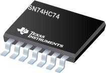
Images are for reference

SN74HC74 Datasheet PDF

Part Series:
SN74HC74 Series
Category:
-
Description:
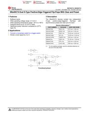
Dual D-Type Positive-Edge-Triggered Flip-Flops With Clear and Preset
Updated Time: 2023/01/13 02:31:59 (UTC + 8)

SN74HC74 Datasheet PDF -

33 Pages
TI
Flip Flop D-Type Pos-Edge 2Element 14Pin SOIC Tube
33 Pages
TI
TEXAS INSTRUMENTS SN74HC74PW Flip-Flop, Complementary, Differential, Positive Edge, 74HC74, D, 15ns, 60MHz, 5.2mA, TSSOP
33 Pages
TI
Flip-Flop, 74HC74, D, 15ns, 60MHz, TSSOP
33 Pages
TI
Flip Flop D-Type Pos-Edge 2Element 14Pin SSOP T/R
33 Pages
TI
Flip-Flop, 74HC74, D, 15ns, 60MHz, 5.2mA, SOIC
33 Pages
TI
Flip Flop D-Type Pos-Edge 2Element 14Pin SSOP T/R
33 Pages
TI
TEXAS INSTRUMENTS SN74HC74PWT Flip-Flop, Differential, Positive Edge, 74HC74, D, 15ns, 60MHz, 5.2mA, TSSOP
33 Pages
TI
TEXAS INSTRUMENTS SN74HC74PWG4 Flip-Flop, D, 15ns, 60MHz, 5.2mA, TSSOP
31 Pages
TI
* Wide Operating Voltage Range of 2V to 6V * Outputs Can Drive Up To 10 LSTTL Loads * Low Power Consumption, 40μA Max ICC * Typical tpd = 15ns * ±4mA Output Drive at 5V * Low Input Current of 1µA Max
31 Pages
TI
Dual D-Type Positive-Edge-Triggered Flip-Flops With Clear and Preset
30 Pages
TI
Flip Flop D-Type Pos-Edge 2Element 14Pin SOIC T/R
25 Pages
TI
Flip Flop D-Type Pos-Edge 2Element 14Pin TSSOP T/R
24 Pages
TI
Flip Flop D-Type Pos-Edge 2Element 14Pin TSSOP T/R
15 Pages
TI
Flip Flop D-Type Pos-Edge 2Element Automotive 14Pin SOIC T/R
14 Pages
TI
Flip Flop D-Type Pos-Edge 2Element 14Pin TSSOP T/R
14 Pages
TI
Flip Flop D-Type Pos-Edge 2Element 14Pin TSSOP T/R

SN74HC74 - TI Specifications

TYPE
DESCRIPTION
Case/Package
SO-14
show more

SN74HC74 - TI Function Overview

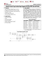
The SNx4HC74 devices contain two independent D-type positive-edge-triggered flip-flops. A low level at the preset (PRE) or clear (CLR) inputs sets or resets the outputs, regardless of the levels of the other inputs. When PRE and CLR are inactive (high), data at the data (D) input meeting the setup time requirements are transferred to the outputs on the positive-going edge of the clock (CLK) pulse. Clock triggering occurs at a voltage level and is not directly related to the rise time of CLK. Following the hold-time interval, data at the D input can be changed without affecting the levels at the outputs.
Wide Operating Voltage Range: 2 V to 6 V
Outputs Can Drive Up To 10 LSTTL Loads
Low Power Consumption, 40-µA Maximum ICC
Typical tpd = 15 ns
±4-mA Output Drive at 5 V
Very Low Input Current of 1 µA
show more
Part Datasheet PDF Search
Loading...
72,405,303 Parts Datasheet PDF, Update more than 5,000 PDF files ervery day.

Relate Parts